Introduction Data acquisition refers to the process of storing, processing, displaying, or printing an analog quantity of temperature, pressure, voltage, current, displacement, flow, etc., after it is converted into a digital quantity. The corresponding system is called a data acquisition system. With the rapid development of computer technology, people are increasingly demanding industrial safety production and modern management. The data acquisition instrument not only needs to collect various sensor signals at the scene, but also sometimes needs to collect and transmit audio and video so that the monitoring personnel can Better control of on-site information. Today, although many high-speed, high-resolution, high-capacity high-performance data acquisition instruments continue to emerge, existing data acquisition instruments still suffer from low CPU frequency and limited processing capabilities. Due to the large amount of data in audio and video signals, it is difficult for a single portable data acquisition instrument to complete the collection and transmission of various sensor signals and audio and video signals in real time. Many data acquisitions use multiple devices for audio, video, and other industrial applications. The sensor signal is collected and transmitted separately. This data acquisition method has disadvantages such as high installation and maintenance costs and large space occupation.
Aiming at the problem that single collectors caused by the low CPU frequency and limited data processing capacity of the current collectors can hardly collect and transmit various signals on the industrial site in real time, a hardware compression encoding scheme for audio and video is proposed. The acquisition instrument carries out the hardware compression coding of the collected audio and video signals in MP3 and H.264 formats, greatly reducing the CPU resource consumption during data processing and the bandwidth occupation during data transmission, and solving the portable data acquisition instrument. It is difficult to realize the integration of multiple data collection and transmission on the industrial site. The collecting instrument integrates a variety of signal acquisition, processing and transmission in the industrial field, and has the advantages of high integration, small size, and strong scalability.
Figure 1 data acquisition instrument structure The overall design of the system is based on the requirements of integrated data acquisition. The acquisition instrument integrates the collection, processing and transmission of multiple data. Its composition is shown in Figure 1. The core processing chip of the data acquisition instrument adopts the 16-bit/32-bit product introduced by Samsung. The RISC microprocessor S3C6410, which has a 64-bit/32-bit internal bus architecture, includes multiple hardware accelerators, and its internal integrated multi-format codec (MFC) supports multiple formats of hardware codecs. In addition, S3C6410 includes many hardware peripherals (such as a camera interface, TFT 24-bit true color LCD controller, system manager, 4-channel UART, 32-channel DMA, general-purpose I / O port, IIS bus interface, IIC bus interface, USB host devices, etc.) greatly reduce the total system design cost and improve system performance. The data acquisition part includes sensor output signals, audio and video signal acquisition. The CPU processes and determines the collected sensor signal. If the signal exceeds the normal range, the data acquisition device sends an alarm and controls the external related device to operate through the GPIO pins of the S3C6410. The scanner has built-in large-capacity NandFlash and SD cards for long-term preservation of signals collected at the scene. In terms of communication, the collector uses the RT3070 wireless communication module produced by Ralink to communicate with the remote monitoring system. The RT3070 module is a USB interface high-speed WIFI module that supports the 802.11n protocol for embedded applications. The wireless communication rate can be up to 150Mbps. . Because in the ARM application, the design of the data display and storage circuit and the serial port and Ethernet communication circuit has been very popular, this article will focus on the hardware design of the data acquisition part.
Sensor signal acquisition industry commonly used analog sensor output signal is 4mA-20mA current and 0-5V voltage. Because the signal transmission process is often distorted by the interference of other electromagnetic waves in the external environment, sometimes the distortion is still very serious, which causes the collector to judge the situation on the spot and direct the machine to malfunction, affecting the company’s production efficiency, and sometimes even causing people’s Life and huge loss of property. Therefore, the collected signal needs to be filtered first. In this design, the industrial output analog signal is first filtered by the filter to high frequency and then sent to the A/D module for analog-to-digital conversion. The converted digital signal is read by the S3C6410 through the SPI interface.
The filter circuit design filter is essentially a process of extracting the information carried by the original signal from the noise-distorted and contaminated signal. The collector filter circuit is shown in Figure 2. Because the filter and the AD conversion signal are voltage signals, a 250Ω precision resistor and a voltage follower are added to the current input. The current signal is first converted to 1V-5V through a precision resistor. The signal then goes through a voltage follower for impedance matching and then enters the filter circuit to filter out high-frequency interference. For voltage input directly into the filter circuit for filtering. In the filter circuit, because the Butterworth response can maximize the passband flatness of the filter, which is especially suitable for low frequency applications, it is very important for maintaining the flatness of the gain, so the design uses Butterworth second-order low-pass filter. The voltage signal is low-pass filtered by a second-order Butterworth filter composed of an LM324 operational amplifier. After the filtering is completed, the signal enters the A/D conversion module for A/D conversion. According to the Butterworth second-order filter characteristics, the cutoff frequency of the filter is: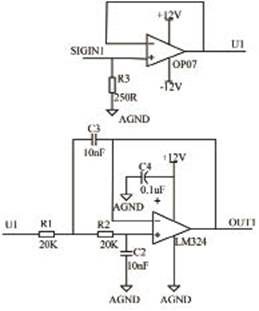
Figure 2 low-pass filter circuit A/D conversion design often needs to convert the analog signal into a digital signal that the processor can recognize in data acquisition, so that the acquisition instrument can process and transmit the signal, which requires an A/D conversion circuit. The principle of A/D converter in terms of transformation is mainly parallel comparison type, successive approximation type and double integral type. The parallel comparison type conversion speed is fast, up to several tens of nanoseconds, but the price is expensive, and it is generally not used when it is not necessary; the conversion time of the double integral type A/D converter is generally 40 ms to 50 ms; the successive approximation type has Higher conversion speeds, up to a few microseconds, are affordable. This design adopts AD7689 chip that ADI Company produces to carry on A/D conversion to the voltage signal after filtering. The AD7689 is an 8-channel, 16-bit resolution, no-loss-code, charge redistribution successive approximation analog-to-digital converter (ADC) powered from a single supply. The AD7689 uses a simple SPI interface to implement the writing of configuration registers and the output of conversion results.
One of the characteristics of audio capture design embedded products is limited CPU resources, in order to reduce the burden on the CPU in the data processing and reduce the bandwidth required for data transmission, the design of the collected audio and video data were separately hardware compression coding. The MAS3587 chip produced by Micronas Semiconductor Design and Manufacturing Company was used for audio acquisition and processing. The chip integrates preamplifier and A/D conversion module, supports analog and digital serial input and output in two ways, and has MPEG1/2layer3 format encoding and MPEG1/2layer2andlayer3 format decoding function. The chip contains a headphone driver module and the analog output signal can directly drive the headphones without amplification. Audio acquisition circuit shown in Figure 4, after receiving the analog signal input, MAS3587 first through the chip A / D part of the analog signal is converted to a digital signal, and then the A / D conversion output digital signal into the chip built-in MP3 The compression encoding module completes the MP3 format encoding. In FIG. 4, S3C6410 initializes the MAS3587 chip through the I2C bus, and reads the audio data encoded by the MP3 format through a handshake signal line and a parallel data line, and stores and transmits the data.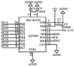
Figure 3 A / D conversion circuit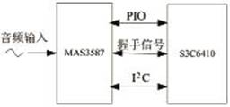
Figure 4 audio capture diagram Other modules design video capture on video capture because the S3C6410 processor integrates a multimedia codec (MFC), supports MPEG4/H.263/H.264 encoding and decoding, and VC1 decoding, providing real-time video conferencing and NTSC And PAL TV output. In addition, the S3C6410 integrates the CameraIF interface and supports the ITU-RBT-601/656YCBC8 8-bit standard with a maximum input size of 4096 x 4096 pixels. This design makes full use of the S3C6410's on-chip resources to complete video capture and hardware compression coding. Video capture is directly connected to the OV9650 camera via the CameraIF interface of the S3C6410 to collect live video data. The built-in MFC module then performs hardware compression encoding of the collected video signals in H.264 format.
WIFI communication communicates with the host computer in a wireless manner. When collecting data, the environmental restrictions are greatly reduced. The wireless data acquisition has the advantages of convenient installation, flexible use, and easy extension. It can change the position of data collection at any time. When uploading data, it is also very Convenience. In order to meet the requirements of real-time transmission of large amounts of data, the acquisition instrument uses the 802.11n protocol to communicate with the host computer. The 802.11n protocol is a wireless transmission standard protocol behind the 802.11a/b/g of the Wi-Fi Alliance. It has faster data transmission speed and stronger signal stability than 802.11a/b/g. The purpose of the protocol is to achieve high-bandwidth, high-quality WLAN services and enable wireless LANs to achieve Ethernet performance levels. Here, we use Ralink RALINKRT3070 high-speed wireless network card, this card driver supports WindowsCE, Linux and other embedded operating systems, compatible with IEEE802.11b/g/n standards, with a small size, signal stability, data transmission speed (up to 150Mbps) and other advantages.
Conclusion This article takes the integration of industrial field sensors and audio and video signals as the research content, and carries out hardware compression coding for the huge amount of audio and video signals, which saves the resource occupation and data transmission bandwidth in the process of CPU data processing. Using the characteristics of high integration and high data processing speed of the S3C6410 processor, a hardware platform for collecting data, collecting, processing, and transmitting physical data is integrated. The collector has the advantages of small size, high integration, stable signal, flexible use, etc. It can be used for data collection and monitoring in underground, power stations, factories and other places, and has broad application prospects.
Aiming at the problem that single collectors caused by the low CPU frequency and limited data processing capacity of the current collectors can hardly collect and transmit various signals on the industrial site in real time, a hardware compression encoding scheme for audio and video is proposed. The acquisition instrument carries out the hardware compression coding of the collected audio and video signals in MP3 and H.264 formats, greatly reducing the CPU resource consumption during data processing and the bandwidth occupation during data transmission, and solving the portable data acquisition instrument. It is difficult to realize the integration of multiple data collection and transmission on the industrial site. The collecting instrument integrates a variety of signal acquisition, processing and transmission in the industrial field, and has the advantages of high integration, small size, and strong scalability.
Figure 1 data acquisition instrument structure
Sensor signal acquisition industry commonly used analog sensor output signal is 4mA-20mA current and 0-5V voltage. Because the signal transmission process is often distorted by the interference of other electromagnetic waves in the external environment, sometimes the distortion is still very serious, which causes the collector to judge the situation on the spot and direct the machine to malfunction, affecting the company’s production efficiency, and sometimes even causing people’s Life and huge loss of property. Therefore, the collected signal needs to be filtered first. In this design, the industrial output analog signal is first filtered by the filter to high frequency and then sent to the A/D module for analog-to-digital conversion. The converted digital signal is read by the S3C6410 through the SPI interface.
The filter circuit design filter is essentially a process of extracting the information carried by the original signal from the noise-distorted and contaminated signal. The collector filter circuit is shown in Figure 2. Because the filter and the AD conversion signal are voltage signals, a 250Ω precision resistor and a voltage follower are added to the current input. The current signal is first converted to 1V-5V through a precision resistor. The signal then goes through a voltage follower for impedance matching and then enters the filter circuit to filter out high-frequency interference. For voltage input directly into the filter circuit for filtering. In the filter circuit, because the Butterworth response can maximize the passband flatness of the filter, which is especially suitable for low frequency applications, it is very important for maintaining the flatness of the gain, so the design uses Butterworth second-order low-pass filter. The voltage signal is low-pass filtered by a second-order Butterworth filter composed of an LM324 operational amplifier. After the filtering is completed, the signal enters the A/D conversion module for A/D conversion. According to the Butterworth second-order filter characteristics, the cutoff frequency of the filter is:
Figure 2 low-pass filter circuit
One of the characteristics of audio capture design embedded products is limited CPU resources, in order to reduce the burden on the CPU in the data processing and reduce the bandwidth required for data transmission, the design of the collected audio and video data were separately hardware compression coding. The MAS3587 chip produced by Micronas Semiconductor Design and Manufacturing Company was used for audio acquisition and processing. The chip integrates preamplifier and A/D conversion module, supports analog and digital serial input and output in two ways, and has MPEG1/2layer3 format encoding and MPEG1/2layer2andlayer3 format decoding function. The chip contains a headphone driver module and the analog output signal can directly drive the headphones without amplification. Audio acquisition circuit shown in Figure 4, after receiving the analog signal input, MAS3587 first through the chip A / D part of the analog signal is converted to a digital signal, and then the A / D conversion output digital signal into the chip built-in MP3 The compression encoding module completes the MP3 format encoding. In FIG. 4, S3C6410 initializes the MAS3587 chip through the I2C bus, and reads the audio data encoded by the MP3 format through a handshake signal line and a parallel data line, and stores and transmits the data.
Figure 3 A / D conversion circuit
Figure 4 audio capture diagram
WIFI communication communicates with the host computer in a wireless manner. When collecting data, the environmental restrictions are greatly reduced. The wireless data acquisition has the advantages of convenient installation, flexible use, and easy extension. It can change the position of data collection at any time. When uploading data, it is also very Convenience. In order to meet the requirements of real-time transmission of large amounts of data, the acquisition instrument uses the 802.11n protocol to communicate with the host computer. The 802.11n protocol is a wireless transmission standard protocol behind the 802.11a/b/g of the Wi-Fi Alliance. It has faster data transmission speed and stronger signal stability than 802.11a/b/g. The purpose of the protocol is to achieve high-bandwidth, high-quality WLAN services and enable wireless LANs to achieve Ethernet performance levels. Here, we use Ralink RALINKRT3070 high-speed wireless network card, this card driver supports WindowsCE, Linux and other embedded operating systems, compatible with IEEE802.11b/g/n standards, with a small size, signal stability, data transmission speed (up to 150Mbps) and other advantages.
Conclusion This article takes the integration of industrial field sensors and audio and video signals as the research content, and carries out hardware compression coding for the huge amount of audio and video signals, which saves the resource occupation and data transmission bandwidth in the process of CPU data processing. Using the characteristics of high integration and high data processing speed of the S3C6410 processor, a hardware platform for collecting data, collecting, processing, and transmitting physical data is integrated. The collector has the advantages of small size, high integration, stable signal, flexible use, etc. It can be used for data collection and monitoring in underground, power stations, factories and other places, and has broad application prospects.
Silent Oil Free Air Compressor
Medical Air Compressor,Dental Air Compressor,Dental Air Compressor Price,Silent Compressor
Air-Compressor,Auto Compressor Co., Ltd. , http://www.liyangcompressor.com